In this tech note, Linkam and Sensofar demonstrate their collaboration in producing an experimental setup for temperature-controlled optical profilometry experiments.
This has historically been a difficult procedure due to imaging issues caused by spherical aberrations. The combination of Linkam's precision temperature control chamber and Sensofar’s Linnik objective lens eliminates these problems and allows accurate measurement of 3D topographic profiles of nanoscale materials.
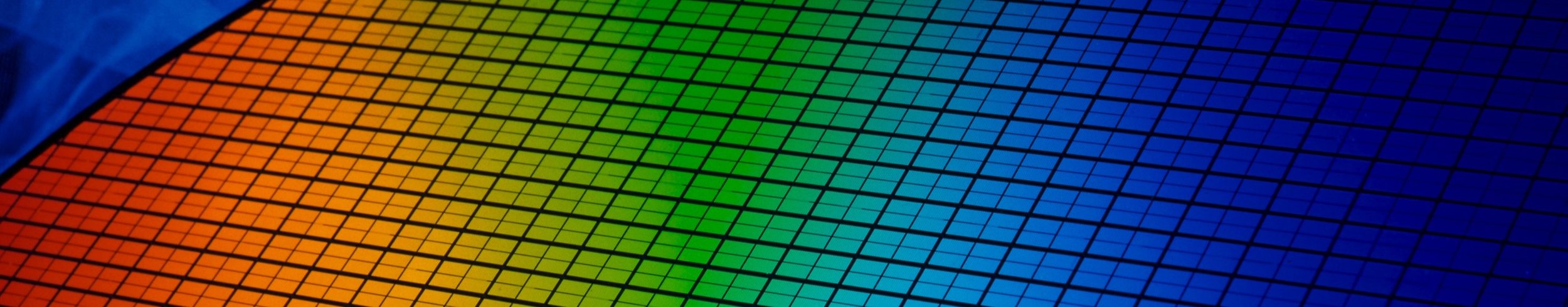
In this application note, we observe the changes in topography of silicon wafers as they evolve with temperature from 20°C up to 380°C.