LTS420

E-skin: Understanding mechanical properties of flexible electronics

LTS420 shown above

Electronic skins (E-skins) that can mimic the functions of a human skin have been intensively studied in the past few years. They are expected to have a great impact on the upcoming generation of portable and wearable electronics related to the Internet of Things. Even after many breakthroughs in the material sciences, there are still difficulties in achieving high performance and highly functional sensors durable enough for continuous monitoring of human activity and health.

Advanced micro- and nanoscale materials within polymer-based protective layers have been successfully applied for the E-skins. However, it is not only important to study and understand the behavior and properties of these electronic materials, but also to create smart structures to achieve the desired performance for these devices.

A research group from University of Oulu in Finland bypassed common performance and functional issues by combining advanced materials and an ingenious structure to achieve mechanosensitivity to different stimuli, high sensing performance, and functionality within the device. The structure not only provided simultaneous ability to be adhered to a human skin or be attached to clothes or textiles, but also possibilities for precise tuning of the response to achieve optimal performances for different locations in the human body. The devices were able to record human activity and health in a reliable manner, providing adequate long-term durability with machine washability.

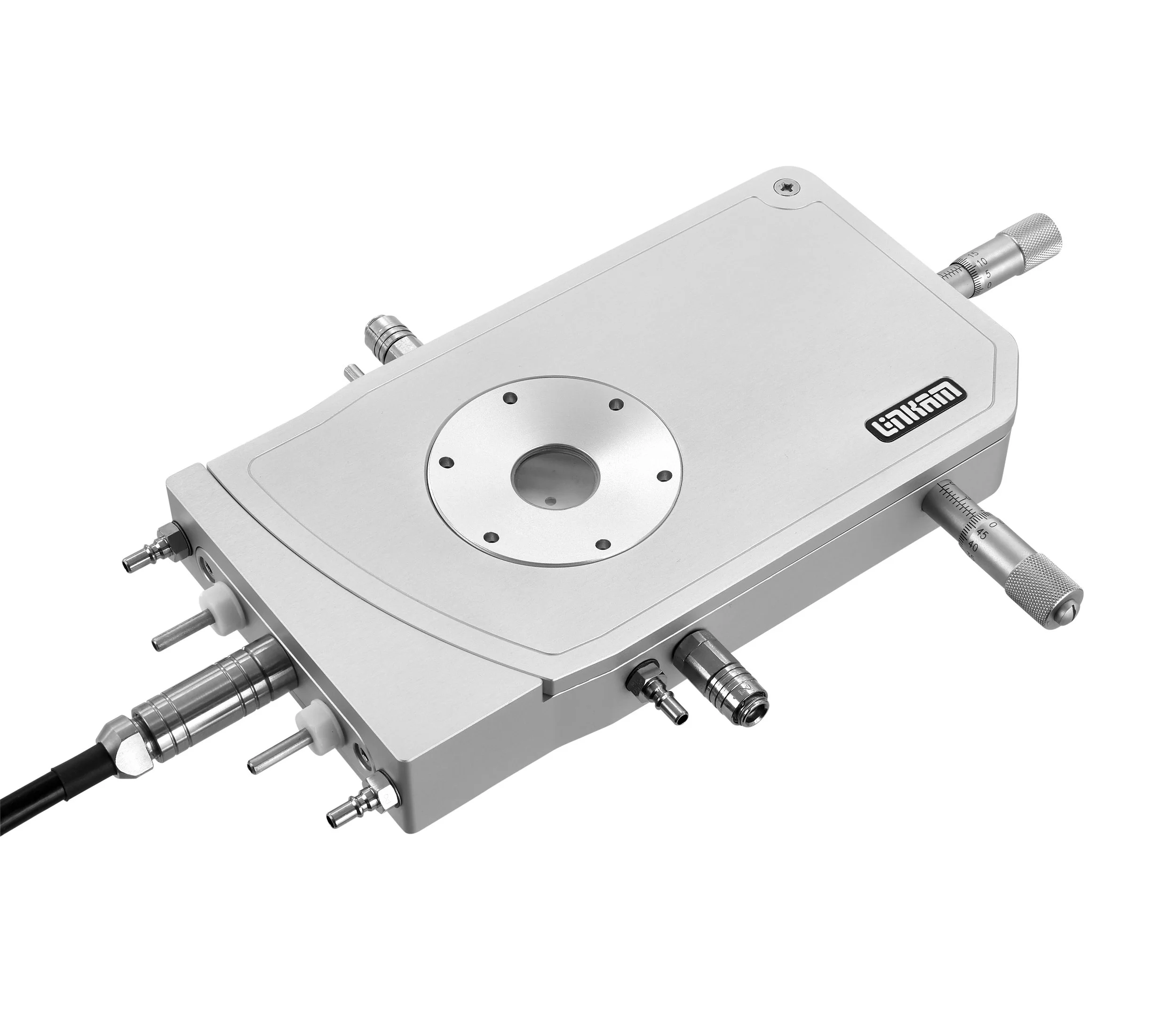
The group used a TST350, now superceeded by the LTS420 to test the tensile properties of their sample. When asked about the purpose of the stage, author Jarrko Tolvanen explained: “In our research the Linkam TST350 stage has provided a reliable way to record the stress-strain curve of various materials. Also, this stage has enabled easy and quick way of testing the mechanical properties under controllable temperature and humidity conditions, that could be proven advantageous when further improving and optimizing the performance of a strain sensor.”

Although more testing is required for long-term durability and environmental stability, the group’s work is a promising start in achieving high performance wearable sensors.

Read the research here

Investigating meniscus-assisted solution printing of large-grained perovskite film for high-efficiency solar cells

LTS420

Solution printing is a novel technique which uses an ink solution, containing semi-conductor precursors or nanoparticles, and deposits these on substrates with desirable characteristics. This offers a cost-effective method of creating large area thin film optoelectronics whilst also offering precise control over the stoichiometry and adaptability of the material. Metal halide perovskites have superb optoelectronic properties and the last few years has seen their power conversion efficiency increase rapidly, largely through the optimisation of the crystal morphology. 

The requirement to control morphology has posed a problem for solution printing. The understanding of crystallisation in dynamic flow of perovskite inks is quite limited, thus imposing restrictions in achieving high-quality perovskite films by the solution-printing technique.

A group from the Georgia Institute of Technology and the University of Nebraska-Lincoln in the USA used a meniscus-assisted solution printing method to elucidate the crystallisation kinetics of perovskite inks and help create high efficiency perovskite solar cells. The thin-films were created with preferred crystal orientation with micrometre-scale grains. 

When discussing their work Professor Lin said, “Through integrating the meniscus effect within the solution printing, we found that the solvent evaporation could be largely promoted by the meniscus effect instead of the thermal evaporation as in conventional doctor-blade coatings, thus leading to the low-temperature solution-based deposition of high-quality perovskite films with preferred crystal orientations. This low temperature feature circumvents thermal degradations and thermomechanical fatigues on perovskite and electrode materials, as well as decreases energy consumptions. Our technique paves the pathway for depositing perovskite thin films on flexible polymer substrates, and is anticipated to promote the future development and applications of perovskites in low-cost, large-area, and flexible optoelectronic devices.”

The group used an LTS350*, now superseded by the LTS420 to control the substrate temperature during the meniscus-assisted solution printing process, due to its capability of precisely controlling the temperature at ±0.1oC. Their investigation on the crystallisation kinetics of perovskite films revealed that a large temperature fluctuation would seriously impact the crystallisation kinetics of perovskite films during the meniscus-assisted printing process. The LTS350* was ideal for maintaining the substrate at a constant temperature and focusing on the exploration of the meniscus effect on the perovskite crystallisation process. 

Their study helped to uncover the crystallisation kinetics of perovskites during the printing process, providing rational guides to precisely control the crystallisation morphology of printed perovskite films. By improving the control over morphology, the group’s work helps to pave a route to large-area optoelectronic devices for commercial applications.

*The LTS350 has been superseded by the LTS420 offering a large temperature range and better temperature control to 0.01°C.

Read the research paper here